
Published: 25 May 2026
Reading Time: 9 minutes
Reviewer: Simon Scrapes, Founder
You know that sinking feeling when one tiny print mistake turns into a whole batch of bad boards? In SMT production, that happens more often than most teams want to admit. A solder paste inspection machine helps catch those issues early, before parts are placed and before reflow locks the problem in.
So, what is solder paste inspection? Put simply, it is the step where a machine checks whether solder paste was printed in the right spot, in the right shape, and in the right amount. This matters because the printing stage sets the tone for everything that follows. If the paste is too high, too low, smeared, or off-center, defects can show up later and cost a lot more to fix.
We have seen that even a small shift in paste position can snowball into rework, line stops, and frustrating quality issues. That is why more teams now want to understand how solder paste inspection machines function, especially as 3D SPI machine technology becomes more common in 2026.
Jace Liu is an experienced manufacturing technology writer specializing in electronics and automation systems. With over a decade of expertise covering industry advancements, Jace brings a wealth of knowledge in surface mount technology solutions.
Why solder paste inspection matters so much
Here is the deal. Most SMT problems do not start at placement or reflow. They start much earlier, right after solder paste printing. If the paste deposit is wrong, the joint built on top of it is usually wrong too.
A solder paste inspection machine checks a few core things:
- Paste volume
- Paste height
- Paste area
- Paste shape
- Paste position and alignment
- Defects like bridging, smearing, offset, too little paste, or too much paste
According to Koh Young America’s overview of solder paste inspection, SPI is used to verify that the right amount of solder paste is in the right place before the board moves forward. That sounds simple. But in real production, it is a big deal.
If you catch a print error before component placement, you save parts, time, labor, and probably a few headaches too. If you miss it, the same board can move into pick-and-place, reflow, test, and maybe even repair. That is expensive.
What is solder paste inspection in practical terms?
Think of SPI as a checkpoint between printing and placement. The board comes out of the printer, the inspection system scans each paste deposit, and the software compares the real print to the expected print.
The machine is not just taking a photo. In many cases, especially with advanced solder paste inspection systems, it is measuring real height and volume data. This helps operators spot issues that a flat image may miss.
In day-to-day use, SPI helps teams:
- Catch print problems early
- Reduce bad boards moving down the line
- Improve first-pass yield
- Feed data back to the printer for better control
- Cut rework and scrap
And yes, this can have a direct effect on throughput. A line that catches defects early usually runs smoother than one that keeps fixing avoidable mistakes later.
2D vs 3D SPI machine technology
Not all systems inspect in the same way. Some older or simpler machines use 2D inspection. Others use 3D SPI machine technology, which is now a common choice for tighter process control in 2026.
Here is a quick comparison:
| Feature | 2D SPI | 3D SPI |
|—|—|—|
| Main view | Flat image | Height and volume measurement |
| Best for | Basic shape and alignment checks | Full paste deposit analysis |
| Accuracy on volume issues | Limited | Much better |
| Defect detection | Surface-level issues | Surface and depth-related issues |
| Fit for modern dense boards | Sometimes | Usually |
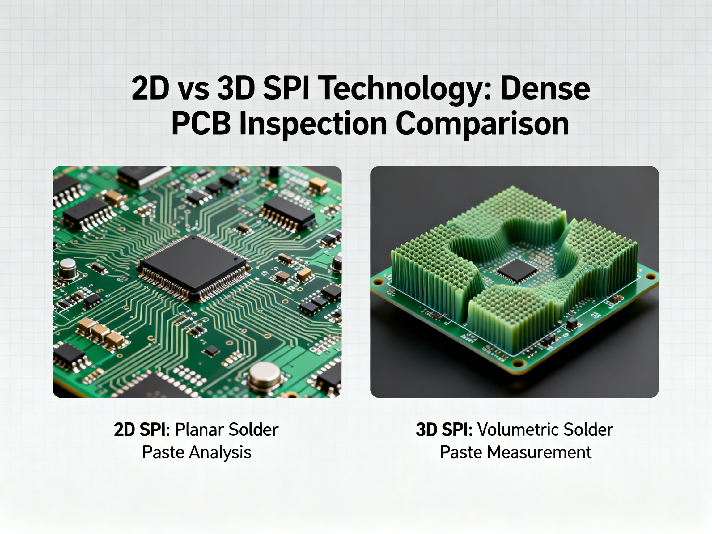
2D systems can still help in simpler production settings. But for fine-pitch boards, dense layouts, and tighter quality targets, 3D SPI machine technology tends to give a clearer picture. Funny enough, this is where a lot of teams realize they were not actually measuring the thing that was causing the defect.
Expert Tip: For the best calibration results, check machine setup against a known good sample board, review height and volume thresholds at the start of each shift, and recheck after stencil changes or paste swaps.
How solder paste inspection machines function
If you have ever asked how solder paste inspection machines function, the answer is pretty straightforward. The machine scans the printed pads, measures each deposit, compares the result to the set limits, then flags anything outside the allowed range.
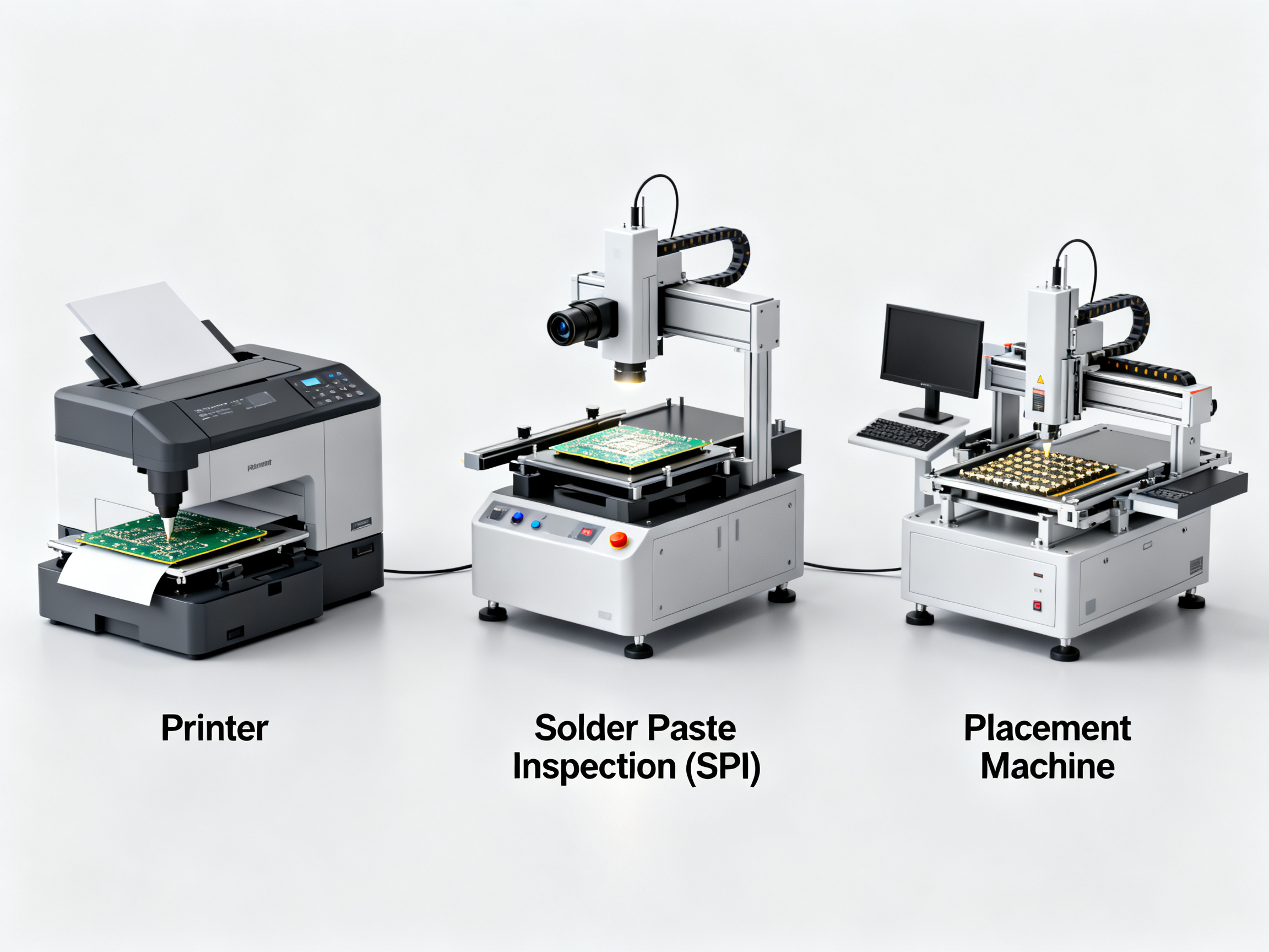
A typical process looks like this:
Step 1: Board enters the SPI station
The printed PCB moves from the stencil printer into the inspection area.
Step 2: The system scans the solder deposits
Depending on the machine, this may use cameras, structured light, lasers, or a 3D measurement method.
Step 3: Software checks the data
The system compares real paste measurements against the programmed model or golden board standard.
Step 4: Defects are flagged
If paste volume, height, area, or alignment falls outside tolerance, the board is marked for review or rejection.
Step 5: Data feeds process improvement
Some lines use SPI results to adjust print settings and keep output more stable over time.
That last point matters a lot. The best SPI setup is not just about finding defects. It is also about learning why they happen.
For production teams planning upgrades, investing in high-quality SPI solutions can support smoother manufacturing lines and reduce costly defects. As advanced 3D SPI machine technology becomes the norm, the future of surface-mount technology is poised for tighter quality control and enhanced process insights.