
Published: 25 May 2026
Reading Time: 12 minutes
Reviewer: [Expert Name Placeholder], [Credentials Placeholder]
Data-Driven Insights on Reflow Temperature Profiles for Optimal Soldering
You know that sinking feeling when a board looks fine coming out of the oven, then fails test an hour later? A lot of teams have been there. Reflow temperature data can look like a dry chart at first, but it often tells the real story behind solder bridges, cold joints, warped boards, and line slowdowns.
In 2026, manufacturers are under more pressure to hit tighter quality targets with less waste. That means reflow soldering profiles are not just a process setting anymore. They are a daily quality tool. If you want better SMT soldering techniques, fewer defects, and stronger output from your reflow soldering process, you need to understand what is reflow temperature profile data actually showing you.
This guide breaks it down in plain language. We’ll cover the profile phases, the optimal soldering temperature range, lead-free vs leaded solder max temperature, ways to measure soldering temperature ramps, and the defect patterns that show up when things drift out of spec. Plus, if you’re reviewing oven upgrades in 2026, this will help you ask smarter questions before you buy.
Jace Liu is an experienced electronics manufacturing engineer with over a decade of experience specializing in SMT (Surface Mount Technology) processes. His career has focused extensively on precision soldering technologies and optimizing production line automation for global EMS and OEM clients.
Understanding Reflow Temperature Profiles: The Basics
So, what is reflow temperature profile, really? It is the full heat path a PCB follows as it moves through the oven. That includes how fast it heats up, how long it stays in each zone, the peak temperature it reaches, and how it cools down.
Most reflow soldering profiles have four main phases: preheat, soak, reflow, and cooling. According to Indium’s overview of reflow phases, each stage plays a direct role in flux activity, wetting, joint formation, and long-term joint strength. Simple chart. Big deal.
Here’s a quick view:
| Phase | What happens | Why it matters |
|—|—|—|
| Preheat | Board temperature rises in a controlled way | Lowers thermal shock and starts flux activation |
| Soak | Heat evens out across the board | Helps remove oxides and prep surfaces for solder flow |
| Reflow | Solder passes melting point and wets pads/leads | Forms the actual solder joints |
| Cooling | Solder solidifies at a controlled rate | Affects grain structure, strength, and final reliability |
I’ve seen teams focus only on peak temperature, then miss the real issue. The ramp and soak sections often cause the trouble first. In my experience, the best profile reviews start before the solder melts. That sounds obvious, but people still skip it when production gets hectic.
Expert Tip: Build a short calibration checklist: confirm thermocouple placement, verify conveyor speed, compare zone setpoints to actual readings, review time above liquidus, and recheck peak temperature on a known-good test board.
The Four Phases, and What Goes Wrong When One Drifts
Let’s make this practical.
1. Preheat
During preheat, the board warms at a steady rate. If the rise is too fast, components can see thermal stress, flux can splatter, and solder balls may show up later. If it is too slow, you lose throughput and may not activate flux well enough.
2. Soak
The soak zone gives the board time to even out. This matters more on dense assemblies with mixed component sizes. A big connector and a tiny chip won’t heat at the same speed, obviously. The soak phase helps narrow that gap.
3. Reflow
This is where solder fully melts and wets the metal surfaces. If peak heat is too low or time above liquidus is too short, the joint may not form well. If both are too high, you can damage parts, burn flux, or raise voiding risk.
4. Cooling
People rush past this one. But the solder reflow cooling stage affects final microstructure and joint reliability. Cooling too fast or too unevenly can stress the assembly. Cooling too slowly can also create grain structures you may not want.
A second source, ProtoExpress on thermal profiling in PCB assembly, points out that poor control in any phase can lead to weak joints, solder balls, and other avoidable defects. So yes, every phase matters.
Optimal Soldering Temperature Benchmark: Leaded vs. Lead-Free Applications
This is where a lot of line teams ask the same thing: what is the optimal soldering temperature range? Fair question. The answer depends on alloy, board design, component sensitivity, and oven behavior.
For leaded solder, common process temperatures are usually around 300 to 320°C at the soldering tool or set process level, with a melting point around 183 to 188°C. Lead-free solder, especially SAC305, often runs around 330 to 350°C in comparable settings, with a melting point near 217°C, based on Piek Training’s guidance on lead-free soldering temperature.
But wait, that does not mean every PCB should hit those numbers as a blanket rule. In reflow soldering profiles, the board-level peak is typically tuned to get reliable melting without overshooting component limits. The machine setpoint and the real board temperature are not always twins. More like cousins.
Here’s a plain comparison:
| Solder type | Approx. melting point | Typical higher process heat needs | Main challenge |
|—|—|—|—|
| Leaded | 183 to 188°C | Lower than lead-free | Easier wetting, but legacy process assumptions can hide drift |
| Lead-free, SAC305 | About 217°C | Higher than leaded | More heat stress, tighter process control needed |
Lead-free vs leaded solder max temperature is not just a materials question. It changes your defect window, board warpage risk, and profile tuning strategy. Lead-free soldering challenges often show up in mixed-mass boards, sensitive packages, and legacy ovens that struggle with tight zone control.
We’ve tested profiles where a lead-free line looked stable on paper, but edge connectors were still underheated while the center was near the limit. That kind of mismatch is common enough to watch for every time you change product mix.
Pro Insight: A common mistake is copying a leaded profile and just adding more peak heat for lead-free boards. That usually backfires. Instead, review ramp rate, soak balance, time above liquidus, and cooling as one linked system.
Lead-Free Transition Problems That Still Catch Teams in 2026
A lot of factories already made the move years ago, but the problems did not vanish. They just changed shape.
Lead-free soldering usually needs more heat, and that can stress laminates, components, and old process windows. Research from ALLPCB on lead-free solder and process performance highlights the higher melting point gap between lead-free and leaded alloys, along with added defect risks like bridging and voids.
That means teams often need to rethink more than just temperature. Flux chemistry, conveyor speed, thermal mass balancing, and oven maintenance all start to matter more. Annoying, yes. But fixable.
If your line is still running older equipment, this is often where newer reflow ovens help. A platform with steadier zone control, better recipe storage, and stronger profiling support can reduce setup drift. For EMS and OEM teams looking at throughput and downtime in 2026, Sun and Mountain SMT’s precision reflow ovens fit naturally into that conversation, especially when the goal is tighter control without rebuilding the whole line.
How to Measure and Optimize Soldering Temperature Ramps
Now for the hands-on part: how to measure soldering temperature ramp without guessing.
The standard setup uses thermocouples, usually Type K, attached to key spots on a real test board. Those sensors feed a multi-channel data logger, and the logger pushes the thermal curve into profiling software. A step-by-step guide from ALLPCB on reflow soldering temperature profiling outlines this workflow clearly.
Here’s the basic process:
- Pick a representative board, not the easiest one.
- Attach thermocouples to hot and cold spots.
- Run the board through the oven at actual line speed.
- Review ramp rate, soak time, peak temperature, and time above liquidus.
- Adjust zone temperatures or conveyor speed.
- Run it again and compare.
That’s the clean version. Real life is messier.
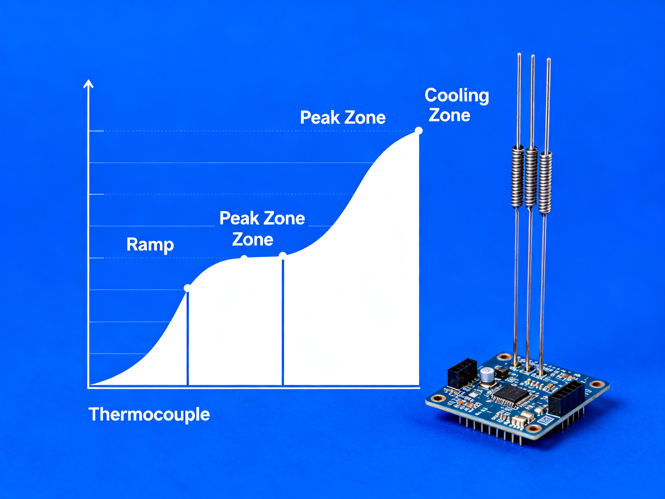
I’ve worked with profiles where one badly placed thermocouple made the whole run look worse than it was. Then we moved the sensor by a few millimeters, reran the board, and the data suddenly made sense. So yes, placement matters a lot.
For electronic manufacturing SMT efficiency, the goal is not just a pretty graph. It is repeatable output with low defect rates over long runs. That’s why smart teams keep a profile library by product family and revalidate after material, stencil, or component changes.
Pro Insight: Use Type K thermocouples, a multi-channel profiler, and software that flags ramp rate, peak, and time-above-liquidus automatically. In 2026, some systems also add AI-based trend alerts, which can help spot drift before defects spike.
Best Tools for Temperature Profiling in 2026
Funny enough, the tool list is not that flashy. But it works.
| Tool | What it does | Best use |
|—|—|—|
| Type K thermocouples | Measure real board temperatures | Capturing hot and cold spots |
| Multi-channel data logger | Records the thermal profile | Comparing zone behavior across the board |
| Profiling software | Turns raw data into usable charts | Tuning ramp, soak, peak, and cooling |
| SPC or line monitoring software | Tracks drift over time | Process control across repeat jobs |
There is also growing interest in AI-driven thermal tuning. An Aivon article on thermal profiling equipment and adaptive control describes how sensor feedback and software can help with predictive adjustments. I would not call AI magic. Not even close. But in 2026, it can save good engineers time by catching trends earlier.
And if your current oven software feels like it belongs on a beige desktop from 1997, that may be part of the problem.
Common Pitfalls and Solder Joint Failures from Incorrect Profiles
This is the part managers usually care about fast, because defects cost money.
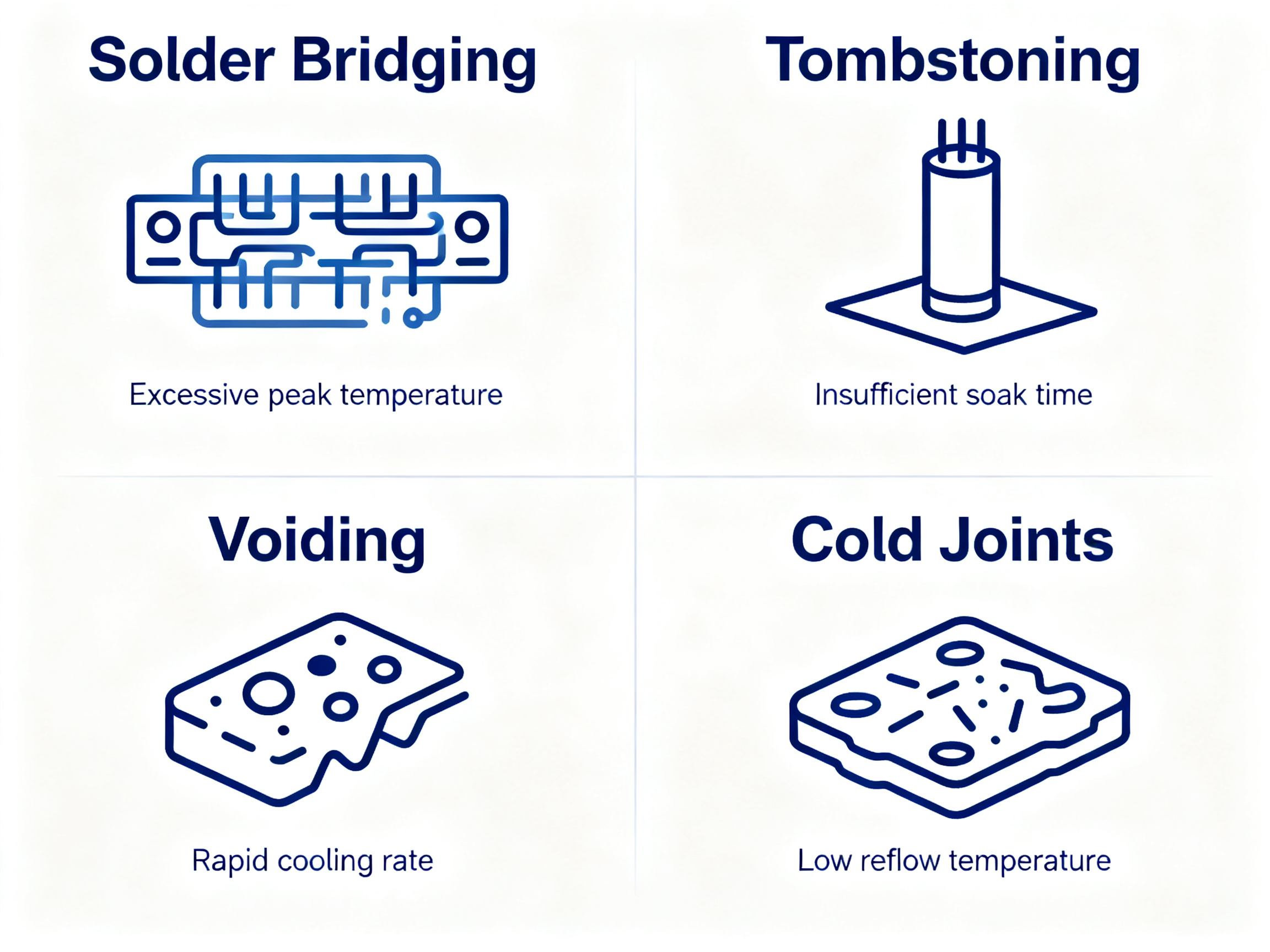
When solder temperature profiles drift, failure patterns tend to show up in a few repeat ways:
- Cold joints from low peak heat or short time above liquidus
- Bridging from excess heat, excess paste activity, or poor soak balance
- Voiding from bad flux outgassing timing or profile mismatch
- Tombstoning from uneven heating across small passive parts
- Component damage from overheating or aggressive ramp rates
- Warped boards from poor thermal balance
So what about solder joint failure rates by temperature? The hard truth is that exact rates vary by alloy, board design, stencil, paste, component mix, and oven stability. There is no single universal chart that gives one perfect defect percentage for every line. But the trend is clear across industry guidance: the farther your profile moves away from the alloy and assembly window, the more failures you tend to see.
We’ve seen this firsthand on dense SMT builds. A profile that looked only slightly hot increased voiding enough to push rework time way up. Not catastrophic at first. Still expensive.
If you are troubleshooting, start with these questions:
- Is the ramp rate too steep?
- Is the soak long enough to balance heavy and light components?
- Is the board actually reaching target peak temperature?
- Is cooling controlled, or just happening however the machine allows?
- Did anything change, even something small, like paste batch or conveyor loading?
That last one gets missed all the time.
Strong reflow control comes from disciplined profiling, verified measurement, and equipment that holds steady under real production pressure. The teams that treat temperature data as a daily operating signal, not a one-time setup task, are usually the ones that ship more reliable boards with less waste.